The electronic technology industry in our world has become modern and more advanced than it was in the past. Printed Circuit Boards (PCBs) in general have helped in the rapid development of this field and have been the reason for making electronic devices more diverse and sophisticated. PCB helped facilitate many aspects of the electronic industries, and that was through many types and shapes of PCB boards. Some of them are simple, single-sided, double-sided, and multiple, but as the complexity of electronic circuits increases, there is a need for High Density Interconnect (HDI) PCB, one of the types that played a role in the development of Electronic industries broadly.
What is HDI PCB?
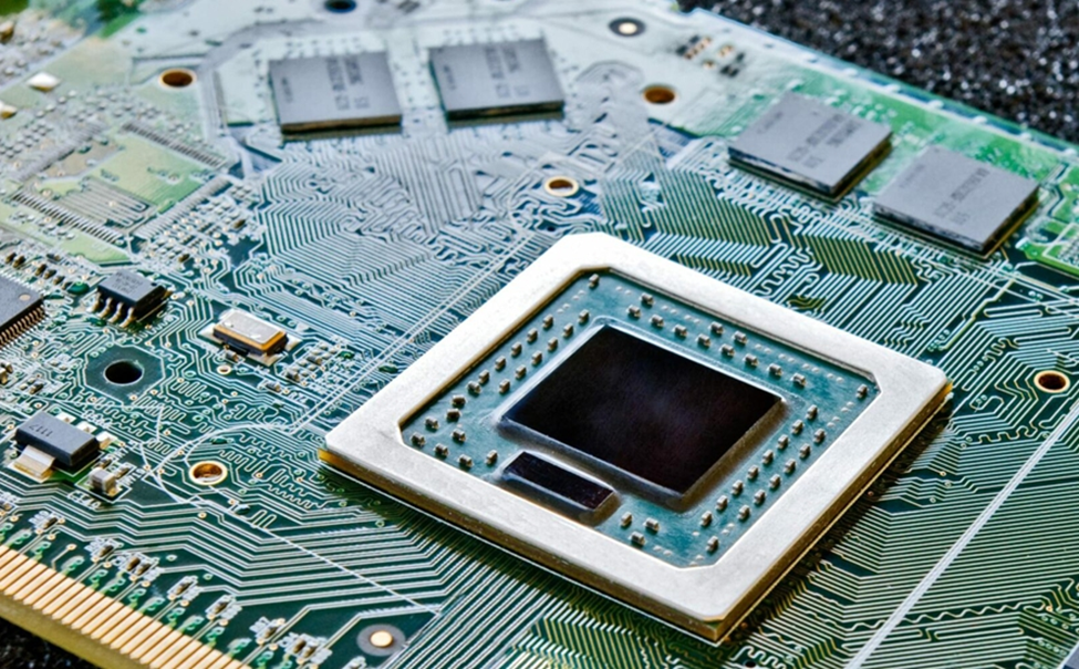
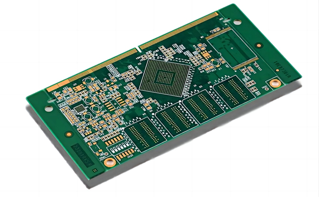
High Density Interconnect (HDI) PCB is a printed circuit board with high wire density, smaller areas, and less thickness than regular PCBs. HDI circuit boards also contain microvias, these small openings that have replaced the regular holes in the traditional PCB. These small ports work to transfer communication between many layers in small spaces. The DHI board also has other types of vias such as buried vias, blind vias, and through hole vias. These different types of vias in the HDI circuit boards made it one of the types of PCB that changed and helped in the advanced electronic industries. It made it possible to manufacture many electronic devices in smaller sizes, lighter weight, and more effective and reliable.
It can be said that HDI multilayer PCB is a multi-layer PCB, but because it contains a high density of wires allows a wide scope for a large number of elements, and thus they can be stacked appropriately without any error occurring.
These panels are widely used in multiple technology fields such as automotive, military, and medical fields. It is characterized by high performance in small spaces, safe signal transmission, and the performance of many tasks with high reliability.
Advantages of High Density Interconnect PCBs
HDI PCB boards are characterized by many advantages that make them superior to their regular PCB counterparts in the field of modern and advanced industries. Some of these advantages are as follows.
- Facilitating the design process: Although the high density interconnect PCB is often used in complex designs, there is freedom in designing and placing many elements because it has a high wire density.
- Transferring the signal quickly and efficiently: The high density interconnect PCB contains different types of vias, and since these holes connect the layers to each other over small and close areas, the rate of signal transfer without any loss or interference is large.
- Integrating a number of complex functions into one board: Due to the small size and light weight of the HDI board, it allows the placement of many components and circuits without taking into account the increase in space or the use of multiple boards. Also, it provides the possibility of adding more components to perform different functions without increasing the size of the PCB board and ensuring its lightweight.
- High performance and economical: the good design of density interconnect PCB allows the possibility of adding many components and performing different functions efficiently and reliably. Since they are small in size, they do not require a lot of raw materials in their manufacture, thus providing the performance of many functions effectively and using fewer materials and one board.
- Power Management: It allows adding more power management elements to the board, which helps ensure improved electrical performance and thus provides reliability and efficiency of performance.
Applications of HDI Printed Circuit Boards
- Automotive: Collision Avoidance system, GPS navigation, consoles, auto drive assistance, ABS and infotainment system
- Industrial Equipment: Control unit, signal module, etc.
- Portable Devices: Smartphones, digital cameras, tablets and other wearable electronics
- Telecommunications: 5G/6G network
- Military Applications
- Medical Facilities
- Aeronautics and Astronautics
- Data Storage Devices and Computing Systems
- High-frequency and High-speed Application Equipment
HDI PCB Manufacturing Process
The HDI PCB fabrication process is considered a complicated process compared to manufacturing regular PCB, so some steps are added to manufacture high density interconnect PCB. Below are some steps for manufacturing high density interconnect PCBs.
- Inner Layer Fabrication: The manufacturing process begins with manufacturing the inner layer, which consists of copper foil, which is engraved and combined with the insulating material.
- Vias Drilling: Microvias are created through the use of advanced techniques such as laser drilling or optical imaging, and these techniques provide high quality and unparalleled accuracy. Creating these slots allows high communication between the layers of the high density interconnect PCB.
- Painting: After the vias drilling process, these holes and their walls are painted, thus creating communication paths between the layers and ensuring the reliability of electrical connections.
- Application Creation: The insulating layers and copper foil are placed one by one around the inner layer, repeating the process of creating microvias and the painting process until the required number of applications is created.
- Stack-up Layers Compacting: Compact the stack-up layers by exposing them to appropriate temperatures and compressing them until they form the structure of the high density interconnect PCB.
- Circuit Printing and Component Placement: Then the electronic circuits are engraved on the outer layer and the components are imprinted.
- Solder Mask and Surface Finishing: The process of finishing the surface and applying the solder mask is done through various finishing techniques, such as Hot Air Solder Leveling (HASL), Organic Solderability Preservative (OSP), and Electroless Nickel Immersion Gold (ENIG). Any of these techniques is used based on the requirements of the application to be manufactured.
- Test and Inspection: Conducting comprehensive tests, such as quality tests through the safety of the electrician’s performance, the integrity of the signal analysis, and other tests that help analyze the board’s performance and efficiency. Finally, a visual inspection process is carried out to ensure the integrity of the produced board and that it is free of any defects using any of the visual detection techniques.
You must have good experience in designing and manufacturing HDI printed circuit boards. The manufacturing process in itself is a sensitive process, so there must be good experience to do it without error. If you do not have experience in manufacturing HDI printed circuit boards, entering such industries without experience will cost significant losses in time and money, so you must have general knowledge of the manufacturing process or the companies that manufacture HDI printed circuit boards.