Industrial control boards are expected to operate for years inside machines that generate heat, vibration, electrical noise, and occasional power disturbances. Unlike consumer electronics, which often operate in relatively predictable environments, industrial controllers may be installed near motor drives, switching contactors, hydraulic equipment, or high-current power distribution systems.
A board can perform perfectly during laboratory testing and still develop intermittent faults after several months in service.
These failures are rarely explained by a single factor. Electrical overstress, thermal cycling, solder joint degradation, environmental contamination, and mechanical stress can interact, creating problems that are difficult to reproduce.
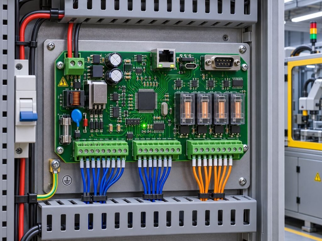
Improving reliability therefore requires more than selecting industrial-grade components. Engineers must understand the physical mechanisms behind failures and verify that the complete assembly can withstand its intended operating conditions.
1. Electrical Transients Can Damage Otherwise Healthy Circuits
Industrial control systems frequently interface with inductive loads such as relays, solenoids, motors, and contactors.
When current through an inductive load changes rapidly, the stored magnetic energy must be dissipated or transferred elsewhere. Without an appropriate current path, a potentially damaging voltage transient can develop.
The fundamental relationship is:
V = L × (di/dt)
where L represents inductance and di/dt describes the rate of current change.
A relay coil, for example, can generate a substantial voltage transient when its current is interrupted.
If the driver circuit lacks suitable suppression, the switching device may experience excessive voltage stress. Transients can also couple into nearby control circuitry through shared impedances or parasitic capacitance.
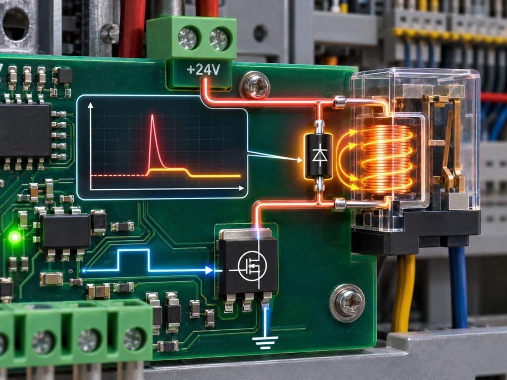
Flyback diodes are commonly used across DC inductive loads. They provide a recirculation path for current when the switching device turns off.
However, a simple diode slows current decay and may increase relay release time.
When faster release is required, a Zener-assisted clamp, TVS device, or another appropriately designed suppression network may be preferable.
Protection selection should account for the load energy, switching frequency, acceptable voltage stress, and required response time.
A TVS diode installed at the wrong location may offer much less protection than expected because PCB trace inductance contributes additional voltage during fast transients.Transient protection is not just a component-selection problem. Its effectiveness depends on where the current flows during the disturbance.2. PCB Layout Can Amplify Switching Noise
Motor controllers and industrial power converters contain current paths with large switching rates.
Even short PCB traces have parasitic inductance. When current changes rapidly, that inductance generates additional voltage.
In a switching loop, the relationship between parasitic inductance and current transition rate directly influences voltage overshoot.
For example, a loop inductance of 20 nH carrying a current transition of 1 A/ns produces an inductive voltage contribution of approximately 20 V.
The actual waveform depends on the circuit, including device characteristics and parasitic capacitances, but the example illustrates why seemingly small layout parasitics matter.
2. High-Current Loops and Return Paths
Power-stage layout should minimize the area of high-di/dt current loops.
Input bypass capacitors must be positioned close to the switching devices they support, with short, low-inductance connections.
Gate-drive loops also deserve attention. Excessive parasitic inductance can contribute to ringing, unintended switching, and increased electromagnetic interference.
Texas Instruments discusses these mechanisms in its application report, Best Practices for Board Layout of Motor Drivers.
Grounding requires similar care.
Sensitive ADC measurements and communication circuits should not share poorly controlled return paths with large switching currents.
However, indiscriminately splitting ground planes can create return-path discontinuities and worsen electromagnetic compatibility.
A continuous reference plane with deliberate current-path management is often preferable, although the appropriate arrangement depends on the system architecture and isolation requirements.
3. Thermal Cycling Gradually Weakens Solder Connections
A board may pass production inspection yet develop electrical failures after repeated heating and cooling.
Industrial equipment commonly experiences temperature changes during startup, shutdown, and normal operation.
Power semiconductors, regulators, and surrounding components also generate localized temperature gradients.
These changes create mechanical strain because the materials within an electronic assembly expand at different rates.
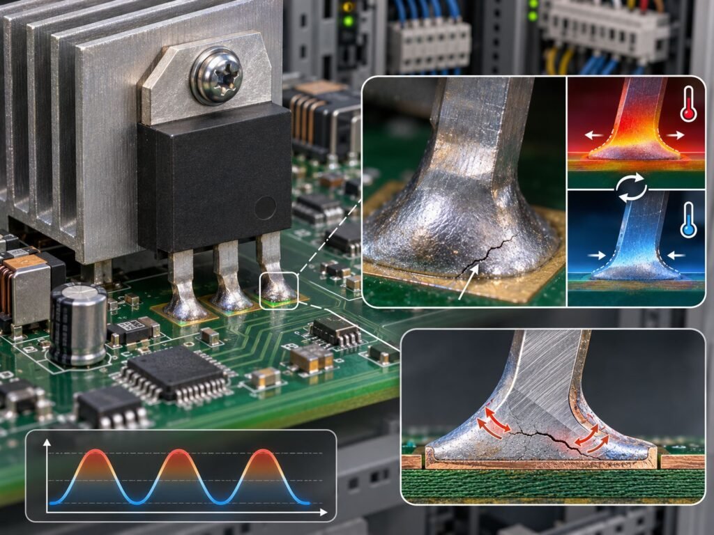
The PCB laminate, copper structures, component package, and solder alloy do not expand identically as temperature changes.
The resulting displacement produces cyclic strain in solder joints.
Over time, plastic deformation and creep can contribute to fatigue crack initiation and propagation.
Large ceramic components and packages with substantial distance from their neutral point can be particularly sensitive to board-level thermal strain.
Cracks may initially cause intermittent connections before progressing into permanent electrical opens.
Why Temperature Monitoring Alone Is Insufficient
A component operating below its maximum junction temperature is not automatically protected against solder fatigue.
Long-term reliability depends on temperature swing, cycle frequency, dwell time, mechanical constraints, and solder joint geometry.
A board cycling repeatedly between 20°C and 90°C may experience different fatigue behavior from one operating continuously near 90°C.
Thermal cycling tests should therefore represent the application’s expected temperature profile rather than relying exclusively on maximum-temperature exposure.
4. Manufacturing Defects Can Become Latent Field Failures
Not all industrial PCB failures originate from environmental stress. Some result from manufacturing defects that remain undetected during initial testing.
Examples include incomplete solder wetting, solder bridges, poorly formed vias, component misalignment, and insufficient solder volume.
Their consequences depend on where they occur and how the assembly is subsequently stressed.
Why Small Assembly Defects Matter
Consider a decoupling capacitor connected to a microcontroller’s power rail.
If one solder joint is partially formed, the capacitor may remain electrically connected under normal conditions but become intermittent during vibration or thermal cycling.
The resulting supply disturbance could cause unexpected resets.
Similarly, a poorly formed via carrying power or a critical signal may pass an initial continuity test but develop increased resistance after repeated thermal stress.
A technical overview of common PCB defects and how to prevent them explains how manufacturing issues such as tombstoning, solder bridging, and via-related defects can affect circuit performance.
The important distinction is between detecting a defect and understanding its consequences.
A visible solder anomaly does not necessarily explain a functional failure. Engineers must establish whether the observed condition can produce the measured electrical symptoms.
Inspection Must Match the Failure Mechanism
Automated optical inspection can identify many visible assembly defects, but it cannot inspect every hidden solder connection.
X-ray inspection may help examine solder joints beneath BGA or QFN packages, particularly when voiding or bridging is suspected.
Cross-sectional analysis can reveal plating discontinuities, interfacial separation, and other structural defects.
Electrical testing adds another perspective, but a board that passes a room-temperature functional test may still contain defects that become apparent under environmental stress.
A strong inspection strategy combines appropriate methods rather than assuming that one technique can detect every potential failure.
5. Moisture and Ionic Contamination Cause Progressive Damage
Industrial electronics are frequently exposed to elevated humidity, condensation, dust, and chemical contaminants.
These conditions become particularly concerning when ionic residues remain on the PCB surface after manufacturing.
Under sufficient humidity and electrical bias, contamination can contribute to electrochemical reactions.
The resulting degradation may include corrosion, increased leakage current, or electrochemical migration.
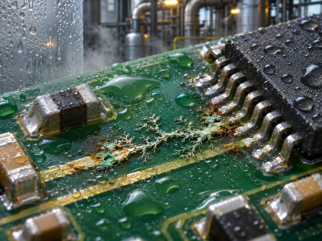
Electrochemical migration can occur when moisture and ionic contamination create an electrically conductive path between biased conductors.
Metal ions may dissolve at one electrode, move through the electrolyte, and deposit elsewhere.
Under suitable conditions, metallic dendrites can form and eventually bridge adjacent conductors.
This process may produce intermittent leakage or a permanent short circuit.
The risk depends on voltage bias, conductor spacing, contamination chemistry, humidity, and exposure time.
The International Electrotechnical Commission discusses these mechanisms and evaluation methods in IEC TR 61191-9:2023, a technical report addressing electrochemical reliability and ionic contamination in electronic assemblies.
Although that document focuses on automotive applications, the underlying mechanisms are also relevant to industrial electronics exposed to moisture.
Why Conformal Coating Is Not a Complete Solution
Conformal coatings can reduce environmental exposure when properly selected and applied.
However, coating does not automatically eliminate contamination-related failures.
Residues trapped beneath a coating may still contribute to leakage or corrosion if moisture penetrates the protective layer.
Coating performance also depends on adhesion, coverage, thickness, material compatibility, and service conditions.
For demanding environments, cleaning validation and coating qualification should be treated as complementary processes.
6. Vibration and Connector Degradation
Industrial equipment can transmit continuous vibration and occasional mechanical shock to electronic assemblies.
These loads may cause solder fatigue, cracked component bodies, or intermittent connector contacts.
Large components are particularly important because their mass can increase mechanical loading during vibration.
A heavy inductor or transformer mounted without sufficient support may impose repeated stress on its solder connections.
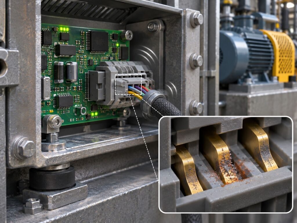
Connectors can fail through a mechanism known as fretting corrosion.
Small repeated movements between contacting surfaces can disrupt protective films and create wear debris.
Depending on the contact material and environment, oxidation and debris accumulation can increase contact resistance.
The resulting symptoms may include intermittent communication errors, voltage drops, or unexpected controller resets.
Simply replacing the connector may restore operation temporarily without addressing the underlying mechanical problem.
Engineers should evaluate connector retention, contact materials, mating cycles, vibration exposure, and cable strain relief.
Board mounting also matters.
Fastener locations, enclosure stiffness, and PCB thickness influence how mechanical loads are distributed across the assembly.
7. Component Derating and Thermal Design
Component selection is another important contributor to industrial reliability.
A component rated for a particular voltage, current, or temperature is not necessarily suitable for continuous operation at its absolute maximum limit.
Engineering derating provides margin against expected operating stresses and uncertainties.
However, derating requirements should be based on the component technology, application conditions, and applicable reliability guidance.
A universal percentage applied to every component is unlikely to provide an optimal design.
Power Dissipation and Junction Temperature
Semiconductor temperature can be estimated using thermal resistance when the assumptions of the thermal model are appropriate.
A simplified steady-state relationship is:
Tj = Ta + P × RθJA
where:
- Tj is junction temperature.
- Ta is ambient temperature.
- P is device power dissipation.
- RθJA is junction-to-ambient thermal resistance.
For example, a device dissipating 2 W with an effective junction-to-ambient thermal resistance of 30°C/W would have an estimated junction temperature rise of 60°C.
At 50°C ambient, the corresponding estimate would be 110°C.
In practice, the effective thermal behavior depends heavily on the PCB construction, copper area, airflow, enclosure, and measurement conditions.
Datasheet thermal resistance values cannot always be transferred directly to a different board layout.
For critical power components, thermal simulation and measurements on representative hardware provide stronger evidence.
8. Manufacturing Quality Must Support the Intended Environment
Reliability requirements should be communicated before PCB fabrication and assembly begin.
An industrial controller installed inside a temperature-controlled cabinet may have very different requirements from a motor control board exposed to vibration, moisture, and elevated temperatures.
The manufacturing process should reflect those differences.
Connecting Design Requirements to Production
Important considerations include laminate selection, copper thickness, hole plating, soldering processes, component moisture sensitivity, and inspection coverage.
For example, a board carrying substantial current may require heavier copper or additional current-carrying structures.
However, heavier copper can affect etching capabilities, minimum trace spacing, soldering behavior, and thermal balance.
These tradeoffs require coordination between the design engineer and the manufacturer.
PCBCool, a PCB manufacturer based in China, describes its work with industrial automation, power electronics, and embedded control applications through its industrial PCB manufacturing services. Such applications illustrate why fabrication capability, assembly controls, and project-specific verification need to be considered together.
Regardless of the supplier, engineers should confirm the actual manufacturing process limits, acceptance criteria, and test requirements for their boards.
Published capability lists are useful starting points, but they do not replace a technical review of the specific design.
9. Environmental Testing Should Target Actual Failure Risks
Testing a controller at room temperature confirms only a limited portion of its expected behavior.
A more meaningful reliability program considers the conditions that the finished equipment will encounter during transportation, installation, and operation.
Depending on the application, this may include temperature cycling, damp heat, vibration, surge immunity, and electrical fast transient testing.
Electrical Immunity Testing
Industrial controllers often connect to long cables or equipment capable of generating electrical disturbances.
Relevant immunity tests may include:
- IEC 61000-4-2: Electrostatic discharge immunity.
- IEC 61000-4-4: Electrical fast transient/burst immunity.
- IEC 61000-4-5: Surge immunity.
The applicable test levels and acceptance criteria depend on the product standard, installation environment, ports, and intended application.
Passing one immunity test does not establish that a product will survive every possible field disturbance.
The purpose of testing is to verify performance against defined requirements and identify weaknesses that require design changes.
Use Test Results to Understand Failure Mechanisms
Environmental testing should produce more than a pass-or-fail result.
If a controller resets during an electrical transient test, engineers should determine whether the disturbance entered through the power input, communication interface, or another coupling path.
If a board fails after thermal cycling, electrical measurements and physical analysis should identify whether the failure involves a solder joint, via, component, or connector.
Without this investigation, corrective actions may address symptoms rather than root causes.
10. Building a More Effective Failure Analysis Process
When an industrial control board fails, replacing the most suspicious component may restore operation without explaining why the failure occurred.
A structured analysis begins by preserving the failed condition and collecting evidence.
Useful information includes operating hours, temperature history, supply conditions, equipment location, and maintenance records.
The next step is to reproduce the electrical symptoms where practical and safe.
Separating Root Cause from Secondary Damage
A failed MOSFET may be the result of a gate-drive problem rather than the original cause of a system failure.
Similarly, a damaged PCB trace may indicate excessive current caused by another component.
Engineers should compare the observed damage against the circuit’s expected current paths and protection behavior.
Measurements should be made with appropriate isolation and safety precautions, especially in equipment connected to hazardous voltages.
Thermal imaging, oscilloscope measurements, insulation resistance testing, microscopy, and controlled component analysis may all contribute useful evidence.
A corrective action should then be validated under conditions capable of reproducing the original failure mechanism.
This is particularly important for intermittent faults that disappear after replacing a component or reheating a solder joint.
Final Thoughts
Industrial control board reliability depends on how electrical, thermal, mechanical, and environmental stresses interact throughout a product’s service life.
The most effective improvements come from identifying credible failure mechanisms early and verifying that the design and manufacturing process can withstand them.
A reliable control board is not simply one that passes its final production test. It is one whose performance remains predictable under the conditions it was designed to survive.
Read Next: